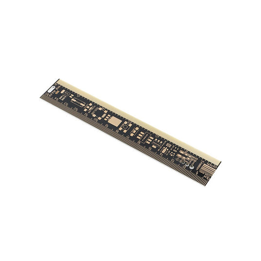


If you solder surface mount components for the first time, you might be surprised: "How small these patch devices are!" They also have many different names! QFN, TDFN, SOIC, SOP, J-Lead, what do these things mean, and how can you tell how big they are? ThinkRobotics offers you a way to handle all of that and much more - a board that you can use as a reference.
This is a handy, stylish PCB reference ruler. Measuring approximately 25.4mm x 152.4mm, with standard thickness of FR4, this gold-plated ruler is engraved with the most common component packages often encountered.
It also has a font size description, a trace width chart, and a set of American Wire Gauge (AWG) drill sizes so you can measure the thickness of your traces at work.
- Material: PCB
- Common line width size reference (unit: mil) 8, 10, 15, 20, 25, 30, 40
- Commonly used drilling diameter reference size (unit: mm) 0.5, 1.0, 1.5, 2.0, 2.5, 3.0
- commonly used resistor-capacitor chip package: 0402, 0603, 0805, 1206, 1210;
- Common MOS, inverter, and triode packages: SOT23, SOT89, SOT25,SOT23-6, SOT223S, SOT254P-6, TO-252;
- Commonly used buttons SW-2, SW-4, miniusb, micro usb, crystal oscillator SM49, TC26, exclusion RES4,
- Device and IC pin spacing comparison table: 0.5mm, 0.8mm, 1.0mm;
- As many as possible include most of the chip IC package formats: TQFP48, TQFP100, TQFP144, SOP20, SOP20_W, SSOP28, SOP8, SOP14, SOP16, SOP8-W, PLCC28, PLCC44, TSOP48, TSSOP24, QFN-16 , BGA100;